ch1
Ch 1: Introduction to GPU Kernels and Hardware
CPU Architecture
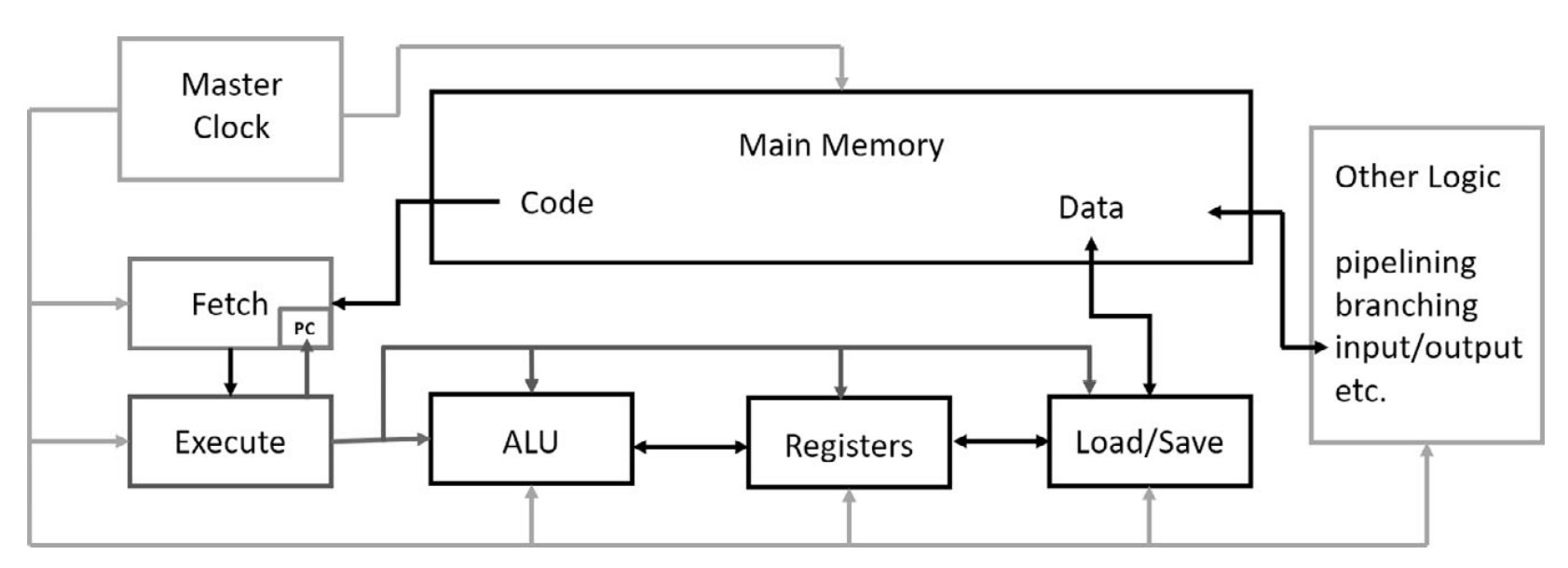
Overview of CPU Components
-
Master Clock
- Controls execution timing with pulses at a fixed frequency.
- Early IBM PCs (1981) ran at 2.2 MHz, increasing over time to 4 GHz (2002).
- Modern Intel CPUs operate at ~3.5 GHz, with short turbo boosts to 4 GHz.
- Power consumption and heat generation increase with frequency.
-
Memory
- Stores program code and data.
- Read operations are handled by the load/save unit or program fetch unit.
- Write operations are usually handled only by the load/save unit.
-
Load/Save Unit
- Reads/writes data between memory and CPU registers.
- Controlled by the execute unit, which determines read/write operations.
-
Register File
- High-speed storage within the CPU for temporary data.
- Data must be in registers before being processed by the ALU.
-
Arithmetic Logic Unit (ALU)
- Performs arithmetic and logical operations on register data.
-
Execute Unit
- Decodes instructions from the fetch unit.
- Manages data transfer to registers and ALU operations.
- Transfers results back to memory.
-
Fetch Unit
- Retrieves instructions from main memory.
- Uses the Program Counter (PC) to track execution.
- Handles branch instructions by updating the PC accordingly.
CPU Memory Management & Latency Hiding
-
Memory Access Latency
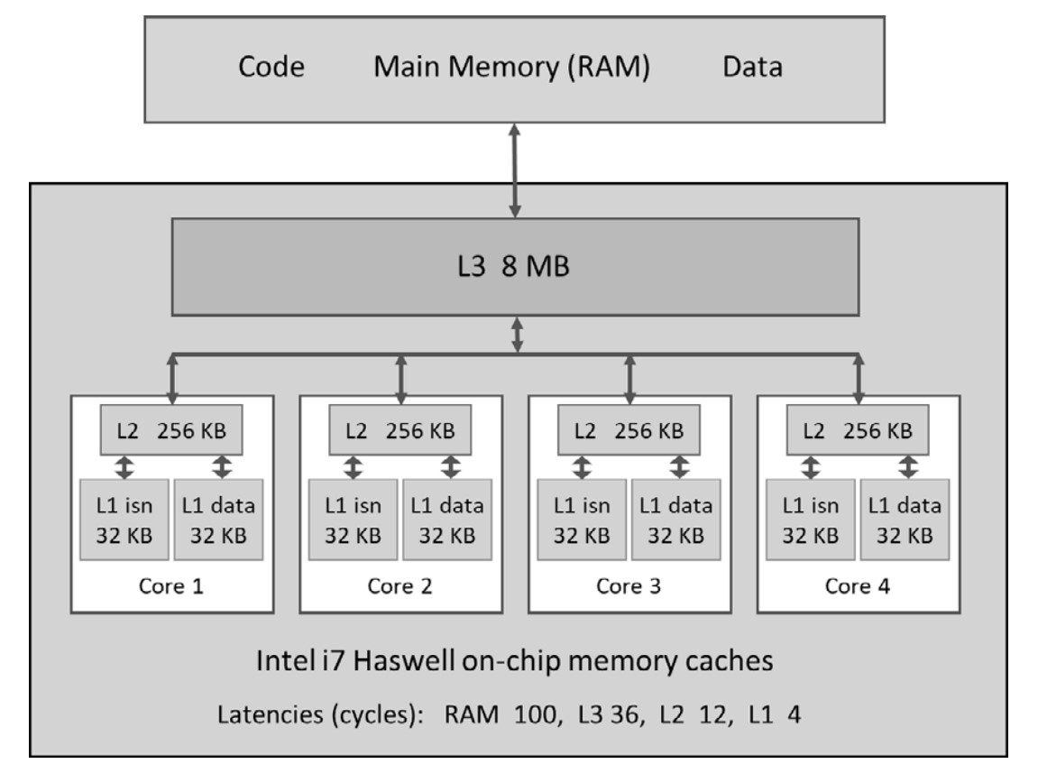
- CPU accesses memory step by step, causing delays.
- Typical CPU memory latency: tens of clock cycles.
- GPU memory latency: hundreds of clock cycles.
-
Caching & Pipelining
- Used to hide latency and improve performance.
- Memory access patterns in loops allow hardware to prefetch adjacent data efficiently.
- Conceptually similar to water flowing through pipes—initial delay, then continuous flow.
-
CPU Cache Hierarchy
- L1 Cache (Fastest, smallest, per-core)
- Separate caches for data and instructions.
- L2 Cache (Larger, slower, per-core)
- L3 Cache (Largest, slowest, shared across cores)
- Cache lines (typically 64 bytes) optimize data transfer efficiency.
- Intel CPUs transfer two adjacent cache lines at once (effective size: 128 bytes).
- L1 Cache (Fastest, smallest, per-core)
- Speculative Execution & Branch Prediction
- Instruction pipelines speed up execution.
- Branch instructions break pipelines, requiring advanced speculative execution.
- The CPU pre-executes multiple potential paths and discards incorrect ones.
3. CPU Parallelism: Vector Instructions (SIMD)
-
Single Instruction, Multiple Data (SIMD)
- Enables parallel processing within a single CPU core.
-
Evolution of Intel SIMD Instructions
- SSE (Pentium III, 1999)
- 128-bit registers, each holding 4× 4-byte floats.
- Aligned data loads/stores allow single-cycle operations.
- AVX2 (Modern Intel CPUs)
- 256-bit registers, supporting more data types.
- AVX-512 (Latest Intel CPUs)
- 512-bit registers, holding 16 floats or 8 doubles.
- Significant speed-up for vectorized computations.
- SSE (Pentium III, 1999)
-
Practical Use of AVX
- Optimizing floating-point computations by processing multiple elements in one instruction.
GPU Origins & Parallel Processing in Graphics
-
Designed for high-performance graphics
- A 1920×1080 screen at 60 Hz requires computing ~125 million pixels per second.
- Each pixel's color is computed independently, making this a massively parallel problem.
- Early CPUs were not powerful enough, leading to the rise of dedicated gaming GPUs.
-
Frame Buffer & Video RAM
- Stores image data in a 2D array, with 3 bytes per pixel (RGB format).
- Specialized video RAM allows simultaneous CPU writes and independent GPU reads for rendering.
General-Purpose Computing on GPUs (GPGPU)
- GPUs evolved from gaming hardware to general-purpose computing tools.
- 2001: GPGPU concept introduced, enabling GPUs for scientific and computational tasks.
- 2007: NVIDIA launched CUDA, making GPU programming mainstream.
NVIDIA GPU Product Lines
-
GeForce (GTX, RTX, Titan) – Gaming GPUs
- Optimized for FP32 (single-precision) calculations.
- Limited FP64 (double-precision) support.
- No ECC (Error-Correcting Code) memory.
-
Tesla – Scientific & Server GPUs
- Designed for high-end scientific computing.
- Strong FP64 support and ECC memory for accuracy.
- No video output ports, unsuitable for gaming.
- Used in server farms and data centers.
-
Quadro – Workstation GPUs
- Tesla-class hardware with added graphics capabilities.
- Targeted at high-end workstations for design, visualization, and scientific applications.
- NVIDIA GPU Generations (2007–2020)
- Each new generation adds more hardware features.
- Generations are named after famous scientists.
GPU Hardware Architecture (Pascal GTX 1080 Example)
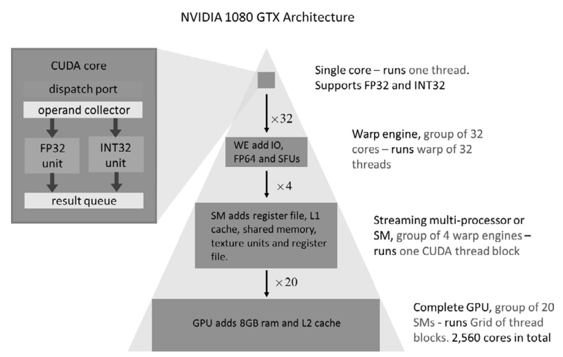
-
Compute Core (Basic Unit)
- Performs 32-bit floating-point & integer operations.
- No individual program counters—executes instructions in groups.
-
Warp Engine (WE) – 32-Core Execution Unit
- Processes 32 threads (warp) in lockstep using one program counter.
- Includes:
- 8 Special Function Units (SFUs) (for fast
sin,exp, etc.). - 1 or 16 FP64 units (for double-precision operations).
- 8 Special Function Units (SFUs) (for fast
-
Streaming Multiprocessors (SMs) – Higher-Level Processing Units
- Each SM has multiple Warp Engines.
- Pascal GPUs:
- 2 (Tesla GP100) or 4 Warp Engines per SM.
- 128 compute cores per SM.
- CUDA thread blocks execute within a single SM.
- Thread blocks within an SM can communicate, but blocks in different SMs cannot.
- Shared memory (96 KB) & L1 cache (24 KB or 48 KB) per SM.
-
Full GPU Structure
- Multiple SMs form the final GPU.
- Example: GTX 1080
- 20 SMs × 128 cores = 2560 compute cores.
- On-chip L2 cache (2–4 GB) shared by all SMs.
-
Different GPU Models for Different Needs
- Gaming GPUs (e.g., GTX 1030) have fewer SMs.
- Differences in clock speed, memory size, and performance.
GPU Processing Model (Warp-Based Execution)**
- Each compute core processes 32-bit data in a stream-like fashion.
- Warp Engine groups 32 cores into a synchronized execution unit.
- Streaming Multiprocessors (SMs) contain multiple Warp Engines.
- Multiple SMs make up the full GPU.
GPU Memory Types & Hierarchical Structure
GPU memory is hierarchically organized, similar to CPU caches, with various levels optimized for different access patterns.
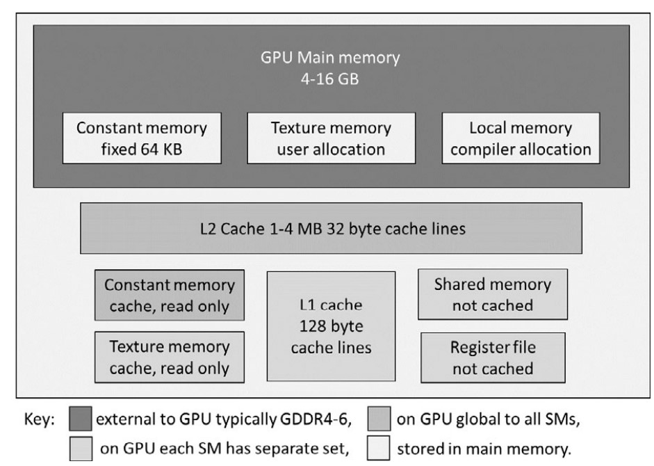
1. Main Memory (Global Memory)
- Equivalent to CPU RAM—stores program code and data.
- Accessible by both CPU and GPU via the PCIe bus (slow, should be minimized).
- Persistent between kernel calls, allowing reuse without reloading.
- Asynchronous memory transfers allow overlapping computation and data movement (useful for tasks like video frame processing).
- Texture & constant memory reside in global memory but have dedicated caches.
2. Constant Memory
- 64 KB reserved in global memory.
- Optimized for read access:
- Dedicated cache bypasses L2, allowing fast access if all threads in a warp read the same value.
- Compiler optimizations:
constandrestricthints help the NVCC compiler automatically use constant memory.- Explicit use is usually unnecessary due to modern compiler optimizations.
- Limited size—not suitable for large data tables.
3. Texture Memory
- Originally for graphics processing, now useful for general-purpose computing.
- Stores 1D, 2D, or 3D arrays optimized for spatial locality.
- Read-only with dedicated texture caches.
- Accessed using special lookup functions:
tex1D,tex2D,tex3D– perform fast interpolation (1D linear, 2D bilinear, 3D trilinear).
- Recent CUDA updates:
- Layered textures (stacks of indexed 1D/2D textures).
- Surfaces (can be written to by the GPU).
- Recommended for image processing and spatial data access.
4. Local Memory
- Private to each thread, used when registers are insufficient.
- Not physically separate—stored in global memory, cached via L1 and L2.
- Automatically managed by the CUDA compiler.
5. Register File
- Each SM has 64K 32-bit registers.
- Registers are shared among thread blocks executing on an SM.
- Performance Consideration:
- An SM supports up to 64 warps (2048 threads).
- If a thread uses more than 32 registers, the number of active threads (occupancy) decreases.
- NVCC option:
--maxrregcount <number>allows manual tuning of register usage vs. occupancy.
6. Shared Memory
- 32 KB – 64 KB per SM (shared among thread blocks on the SM).
- Fast and useful for intra-thread block communication.
- Memory allocation:
- Can be defined at compile time or dynamically at kernel launch.
- If a kernel requests more than half of shared memory, only one block can run per SM, reducing occupancy.
- Performance Trade-Off:
- Early GPUs had poor caching, so shared memory was heavily used to avoid slow global memory accesses.
- Modern GPUs have better L1/L2 caching, reducing the need for shared memory optimization.
- Use shared memory judiciously—balance faster memory access against occupancy reduction.
7. Memory Coalescing & Access Optimization
- Caches (L1 & L2) + high occupancy help hide global memory latency.
- Memory coalescing:
- Optimal pattern: 32 threads in a warp should access 32-bit variables in adjacent memory locations.
- Starting address should be aligned on a 32-word boundary.
- Early CUDA versions emphasized coalescing due to poor caching.
- Modern GPUs are more forgiving, but aligned and sequential memory access remains best practice.
Key Takeaways
- Minimize global memory access—use registers and shared memory where possible.
- Use constant memory for small read-only datasets accessed by all threads.
- Texture memory is beneficial for interpolations and spatial access patterns.
- Too many registers per thread reduces occupancy—use NVCC flags to tune it.
- Shared memory speeds up intra-block communication, but excessive use can hurt occupancy.
- Memory coalescing improves caching efficiency, reducing global memory latency.
GPU Memory Types & Hierarchical Structure
GPU memory is hierarchically organized, similar to CPU caches, with various levels optimized for different access patterns.
1. Main Memory (Global Memory)
- Equivalent to CPU RAM—stores program code and data.
- Accessible by both CPU and GPU via the PCIe bus (slow, should be minimized).
- Persistent between kernel calls, allowing reuse without reloading.
- Asynchronous memory transfers allow overlapping computation and data movement (useful for tasks like video frame processing).
- Texture & constant memory reside in global memory but have dedicated caches.
2. Constant Memory
- 64 KB reserved in global memory.
- Optimized for read access:
- Dedicated cache bypasses L2, allowing fast access if all threads in a warp read the same value.
- Compiler optimizations:
constandrestricthints help the NVCC compiler automatically use constant memory.- Explicit use is usually unnecessary due to modern compiler optimizations.
- Limited size—not suitable for large data tables.
3. Texture Memory
- Originally for graphics processing, now useful for general-purpose computing.
- Stores 1D, 2D, or 3D arrays optimized for spatial locality.
- Read-only with dedicated texture caches.
- Accessed using special lookup functions:
tex1D,tex2D,tex3D– perform fast interpolation (1D linear, 2D bilinear, 3D trilinear).
- Recent CUDA updates:
- Layered textures (stacks of indexed 1D/2D textures).
- Surfaces (can be written to by the GPU).
- Recommended for image processing and spatial data access.
4. Local Memory
- Private to each thread, used when registers are insufficient.
- Not physically separate—stored in global memory, cached via L1 and L2.
- Automatically managed by the CUDA compiler.
5. Register File
- Each SM has 64K 32-bit registers.
- Registers are shared among thread blocks executing on an SM.
- Performance Consideration:
- An SM supports up to 64 warps (2048 threads).
- If a thread uses more than 32 registers, the number of active threads (occupancy) decreases.
- NVCC option:
--maxrregcount <number>allows manual tuning of register usage vs. occupancy.
6. Shared Memory
- 32 KB – 64 KB per SM (shared among thread blocks on the SM).
- Fast and useful for intra-thread block communication.
- Memory allocation:
- Can be defined at compile time or dynamically at kernel launch.
- If a kernel requests more than half of shared memory, only one block can run per SM, reducing occupancy.
- Performance Trade-Off:
- Early GPUs had poor caching, so shared memory was heavily used to avoid slow global memory accesses.
- Modern GPUs have better L1/L2 caching, reducing the need for shared memory optimization.
- Use shared memory judiciously—balance faster memory access against occupancy reduction.
7. Memory Coalescing & Access Optimization
- Caches (L1 & L2) + high occupancy help hide global memory latency.
- Memory coalescing:
- Optimal pattern: 32 threads in a warp should access 32-bit variables in adjacent memory locations.
- Starting address should be aligned on a 32-word boundary.
- Early CUDA versions emphasized coalescing due to poor caching.
- Modern GPUs are more forgiving, but aligned and sequential memory access remains best practice.
GPU Memory Key Takeaways
- Minimize global memory access—use registers and shared memory where possible.
- Use constant memory for small read-only datasets accessed by all threads.
- Texture memory is beneficial for interpolations and spatial access patterns.
- Too many registers per thread reduces occupancy—use NVCC flags to tune it.
- Shared memory speeds up intra-block communication, but excessive use can hurt occupancy.
- Memory coalescing improves caching efficiency, reducing global memory latency.
Warps and Waves in CUDA Programming
1. Importance of Choosing the Right Number of Threads (Nthreads)
- The number of threads (
Nthreads) is problem-specific and crucial for performance. - A good rule of thumb is to maximize
Nthreadsfor full GPU utilization. - Examples:
- For a 1D sum computation with
10⁹steps → use10⁹threads. - For image processing with
nx × nypixels → useNthreads = nx × ny.
- For a 1D sum computation with
2. Misconception: Nthreads = Ncores is Sufficient
- Reality: A GPU hides memory and execution latencies by rapidly switching between threads.
- More threads than cores are needed to keep the GPU fully occupied at all times.
3. Example: CUDA Execution Model on an RTX 2070 GPU
- Hardware Breakdown:
- Streaming Multiprocessors (SMs):
Nsm = 36 - Warps per SM:
Nwarp = 2 - Threads per warp:
32 - Total CUDA cores: [ Ncores = Nsm × Nwarp × 32 = 36 × 2 × 32 = 2304 ]
- Resident Threads per SM (
Nres):1024(i.e., 32 warps per SM) - Active Warps per SM:
2(remaining 30 warps are suspended, waiting for memory).
- Streaming Multiprocessors (SMs):
4. Latency Hiding & Thread Execution in Waves
- CUDA processes threads in waves to maximize GPU utilization.
- Wave Size (
Nwave): $$ Nwave = Nres × Nsm = 1024 × 36 = 36864 \text{ threads per wave} $$ - If launching
10⁹threads:- Total waves required: $$ 10⁹ \div Nwave = 10⁹ \div 36864 ≈ 27127 \text{ waves} $$
- Last wave may be incomplete if
Nthreadsis not a multiple ofNwave.
- Best practice: Set
Nthreadsto at leastNwaveand preferably a multiple ofNwave.
5. GPU Model Variations & Impact on Nwave
- Turing GPUs (e.g., RTX 2070, RTX 2080):
- Resident threads per SM (
Nres):1024 - Example (
RTX 2080):Nsm = 46→Nwave = 1024 × 46 = 47104
- Resident threads per SM (
- Other recent NVIDIA GPUs:
Nres = 2048(double Turing’s value).- Same
Nwarp = 2, butNwavedoubles due toNresincrease. - Varies by model—higher
Nsm→ largerNwave.
Key Takeaways
- Choose
Nthreadswisely—large enough to utilize full GPU potential. - GPU latency hiding is achieved by keeping many resident threads ready to run.
- Threads execute in "waves" (
Nwave), and optimalNthreadsis a multiple ofNwave. - Different GPU models have different
NsmandNres, affectingNwavesize.
Blocks and Grids in CUDA
1. Thread Blocks: Basic Concept
- Thread blocks are groups of threads that execute together on the same Streaming Multiprocessor (SM).
- Key properties:
- Threads within a block can communicate via shared or global memory.
- Threads in different blocks cannot communicate during kernel execution.
- Synchronization is only possible within the same block, not across blocks.
- Thread block size recommendations:
- Must be a multiple of warp size (32).
- Maximum size per block: 1024 threads.
- Common choice: 256 threads per block (submultiple of 1024).
2. Thread Execution on SMs
- An SM can hold multiple thread blocks at the same time.
- Example:
- If block size is 256 threads, up to 4 thread blocks can be assigned per SM (since 1024 / 256 = 4).
- On non-Turing GPUs, up to 8 thread blocks may coexist on an SM.
- Even if multiple thread blocks coexist on the same SM, they cannot communicate with each other.
3. Kernel Launch Configuration: Grid & Blocks
- CUDA kernels are launched with two key parameters:
- Thread block size (
threads) - Number of thread blocks (
blocks)
- Thread block size (
- Total threads (
Nthreads): $$ Nthreads = threads × blocks $$ - Choosing
blocksto match problem size (N):-
Ensure that
Nthreads ≥ N(total threads must be at least the required number). -
If
Ndoes not evenly divide bythreads,blocksmust be rounded up. -
Example:
blocks = (N + threads - 1) / threads; -
Some extra threads may be created, so out-of-range checks are needed in kernel code (e.g.,
if (threadIdx.x >= N) return;).
-
4. Waves & SM Assignment
- NVIDIA documentation does not focus much on waves, but a 2014 blog post by Julien Demouth (link) mentions that threads are dispatched in complete waves when possible.
- Optimizing Grid Configuration:
- Ensure
blocksis a multiple of the number of SMs (Nsm) for best performance. - This helps avoid uneven thread distribution across SMs, reducing the "tail effect" (when some SMs remain underutilized at the end of execution).
- Ensure
Key Takeaways
- Thread blocks execute on one SM and can communicate via shared memory.
- Optimal thread block size: Multiple of 32, typically 256 or 512.
- SMs can process multiple thread blocks at the same time, but blocks do not communicate.
- Kernel launch requires specifying
threadsandblocks:Nthreads = threads × blocks.blocksshould be rounded up to cover the requiredN.
- "Waves" optimize execution—
blocksshould be a multiple of SM count (Nsm) for better load balancing.
CUDA Thread Indexing Variables
| Variable | Description |
|---|---|
threadIdx.x |
Thread rank within a block (0 to blockDim.x - 1). |
blockIdx.x |
Block rank within the grid (0 to gridDim.x - 1). |
blockDim.x |
Number of threads in one block. |
gridDim.x |
Number of blocks in the grid. |
warpSize |
Number of threads in a warp (always 32 on current NVIDIA GPUs). |
| Thread rank in block | id = threadIdx.x |
| Thread rank in grid | id = blockDim.x * blockIdx.x + threadIdx.x |
| Total number of threads | threads = gridDim.x * blockDim.x |
CUDA Occupancy & Resource Constraints
1. Definition of Occupancy
- Occupancy = (Number of resident threads in SM) / (Maximum resident threads
Nres). - Expressed as a percentage.
- 100% occupancy means that complete waves are running on all SMs.
2. Factors Affecting Occupancy
Even if enough threads are launched for full occupancy, other hardware constraints may reduce actual occupancy:
- Register Limitations
- NVIDIA GPUs allow up to 32 registers per thread while maintaining full occupancy.
- Excess register usage reduces active threads per SM, lowering occupancy.
- Shared Memory Limitations
- Non-Turing GPUs: 64 KB or 96 KB per SM → 32 or 48 bytes per thread at full occupancy.
- Ampere GPUs: Increased to 80 bytes per thread at full occupancy.
- High shared memory usage reduces the number of resident thread blocks, lowering occupancy.
3. Performance Considerations
- Lower occupancy is not always bad—acceptable in compute-bound kernels.
- Memory-bound kernels benefit from higher occupancy to hide memory latency.
- Optimization strategies:
- If shared memory usage is too high, consider using global memory and relying on L1 caching instead.
- Experimentation is required to find the best balance between occupancy and resource usage.